Nanoscale Magnetometry of 2D Materials
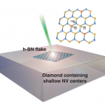
In the Lukin group, we use nanoscale magnetometry based on diamond NV spin qubits to probe the magnetic fields coming from spins and electrical currents in 2d materials.
2d materials come from layered parent compounds which can be mechanically exfoliated to isolate single-atom thick monolayers. Famous examples include graphene, hexagonal boron nitride and transition metal dichalcogenides. This exciting new class of materials feature a wide variety of electronic and magnetic properties which behave completely differently in the 2d limit.

One challenge in the study of 2d materials is the limitation of traditional bulk measurement techniques – the signals are just too small coming from the tiny material volumes. To tackle this problem, we use the diamond NV spin qubits to detect the magnetic fields emanating from 2d materials. This approach opens a wide experimental platform for studying the behavior of spins and electrons on the nanoscale.
References:
I. Lovchinsky et. al., Science 355, 6324: 503-507 (2017).